Minyang New Energy(Zhejiang) Co., Ltd.

Call Us Today!

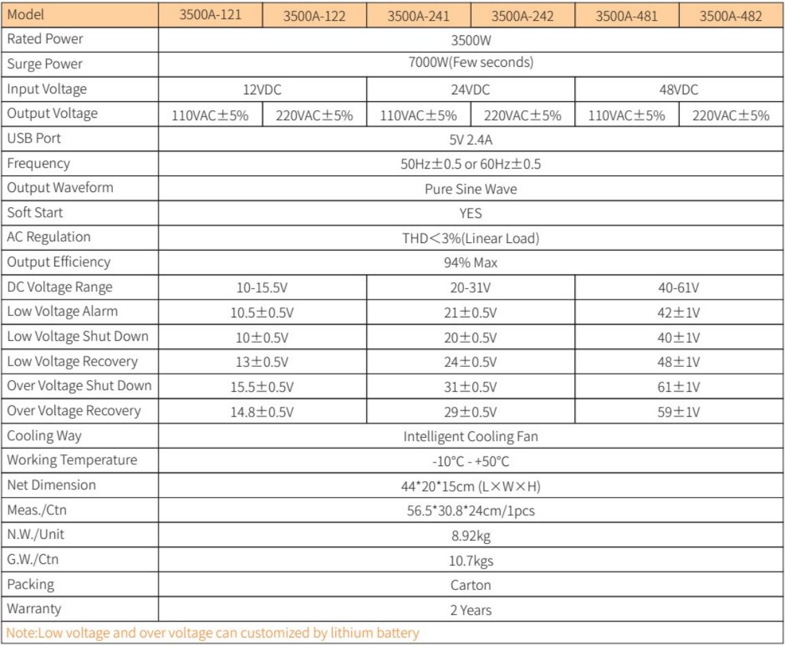
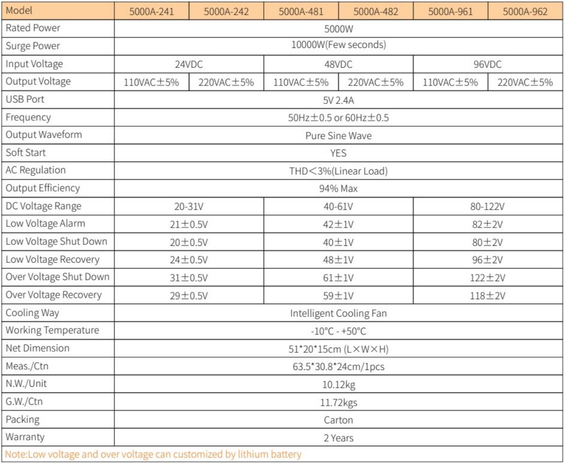
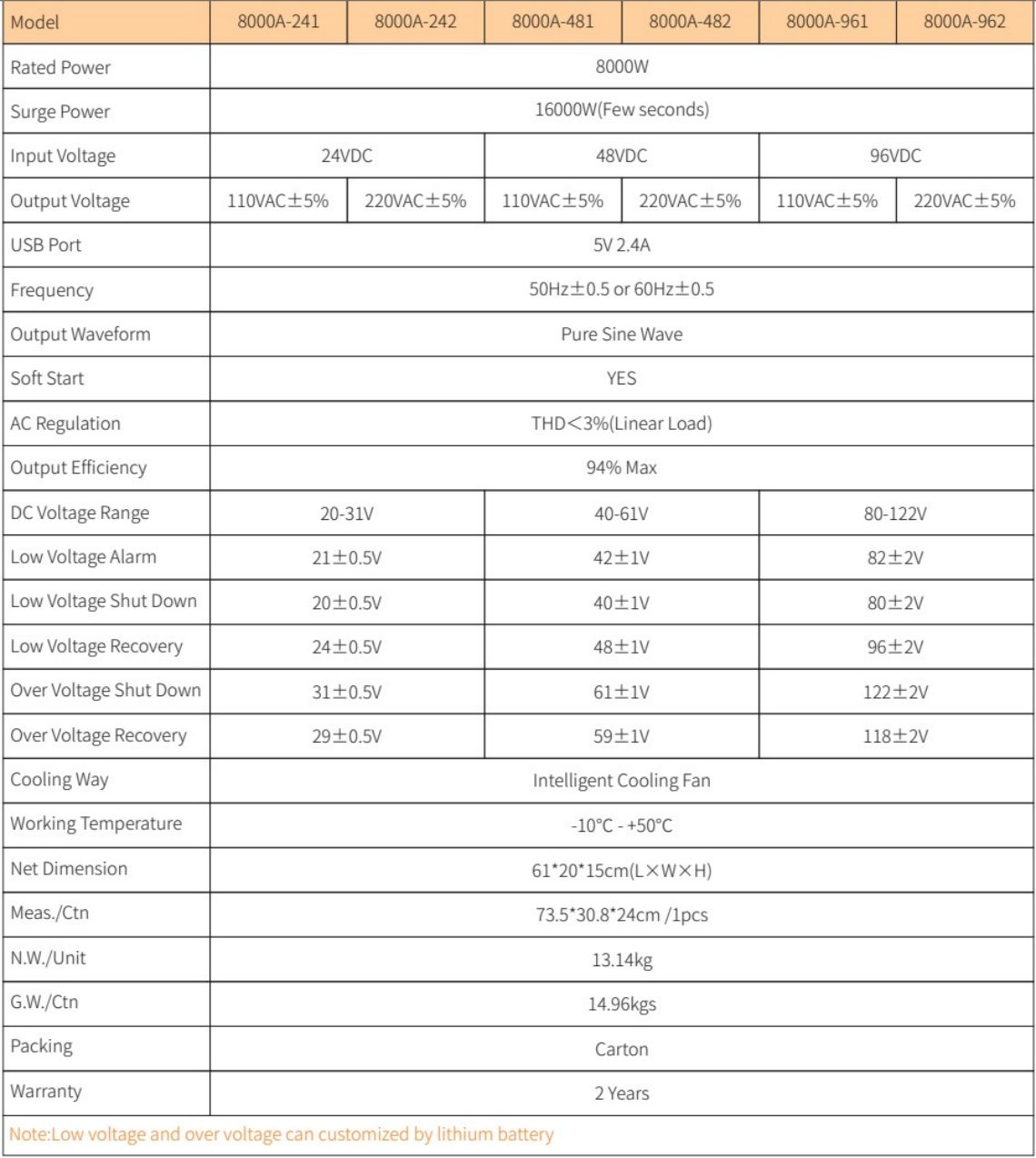
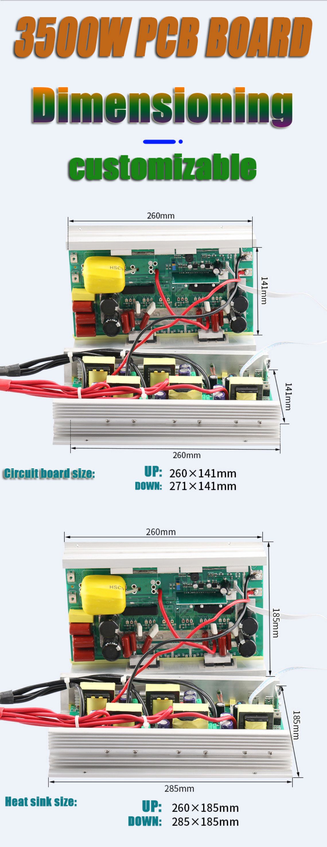
China manufacturer SGP-2000-8000W 110/220VAC 12v 24v 48v sine wave inverter pcb board solar hybrid inverter pcb board

Short Description:

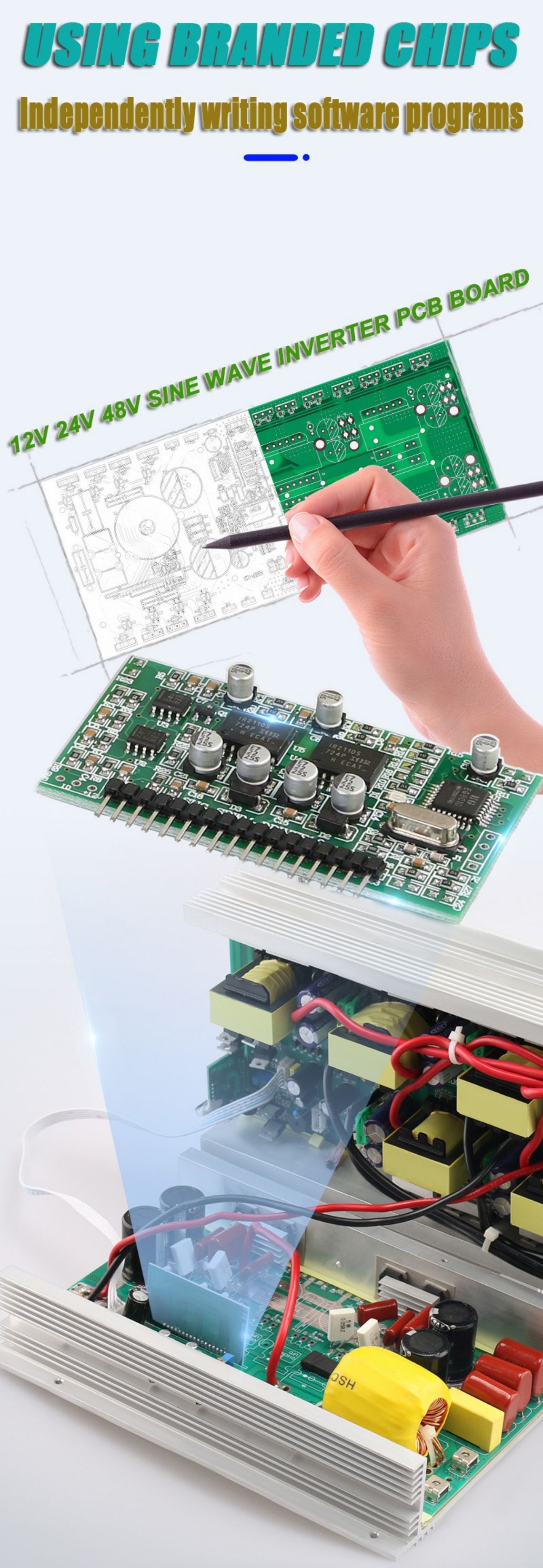
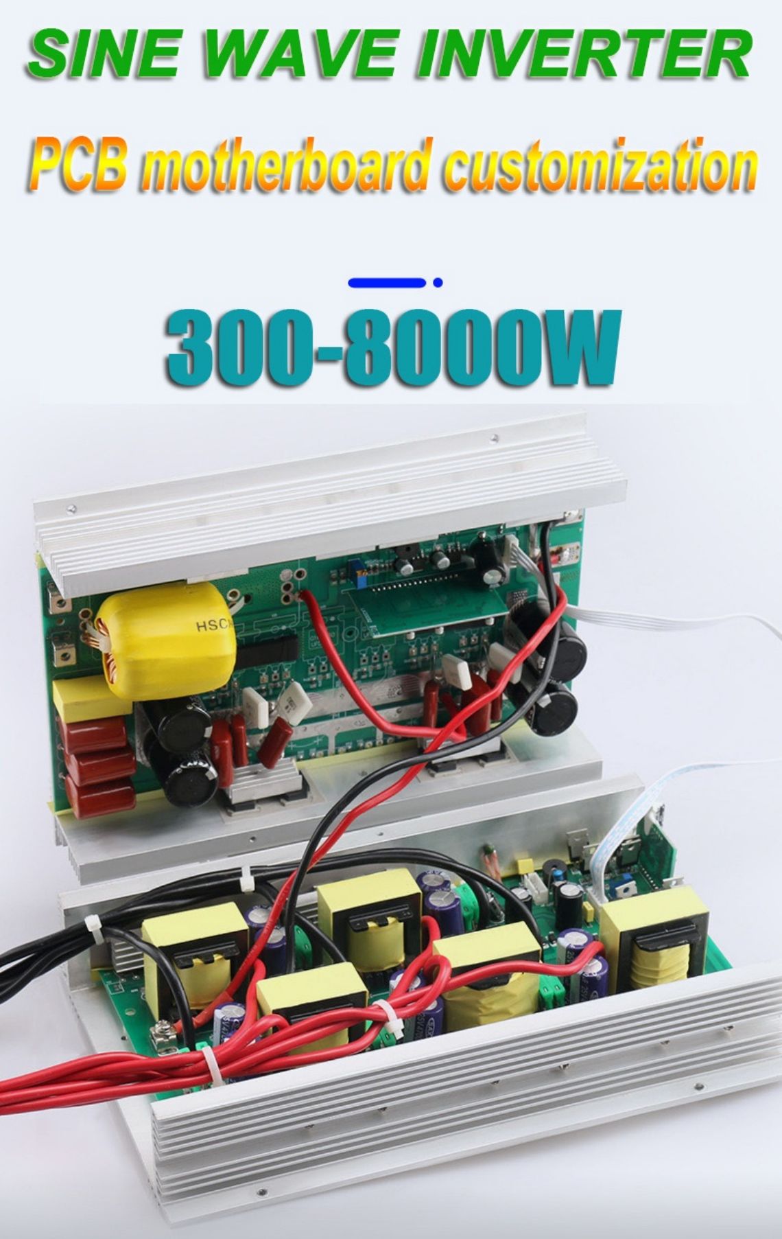
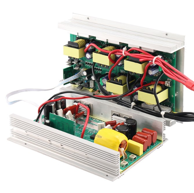
The inverter PCB board is the main component of the inverter circuit board, and its original process is a very important part of the inverter production. The process of connecting electronic components to the inverter circuit board in the correct way is the process of the original inverter PCB board. This job requires a high level of technical proficiency and professional knowledge, as correct connection is crucial, not only to ensure the efficiency and reliability of inverter operation, but also to ensure that the inverter operates within a safe range.

Product Detail

Product Tags

Product description

The inverter PCB board is the main component of the inverter circuit board, and its original process is a very important part of the inverter production. The process of connecting electronic components to the inverter circuit board in the correct way is the process of the original inverter PCB board. This job requires a high level of technical proficiency and professional knowledge, as correct connection is crucial, not only to ensure the efficiency and reliability of inverter operation, but also to ensure that the inverter operates within a safe range.

Inverter circuit board,PCB

Product features

1. Design circuit diagram
Before starting the production of the inverter PCB board, it is necessary to design the circuit diagram and determine the required electronic components and other components. Designing circuit diagrams requires professional technical and software support, usually completed by engineers or electronic experts.
2. Layout
Layout refers to the process of placing electronic components on the inverter PCB board, which is one of the Committed step in the production of inverter PCB board. The correct layout can better organize electronic components and other components, making them easy to operate and maintain during welding. There are many ways of layout, which should be laid out reasonably based on the design of the circuit diagram and the actual situation.
3. Welding
Welding is the final step in the process of inverter PCB components. The purpose of welding is to weld electronic components together with the solder pads on the inverter PCB board, ensuring stable and reliable connection and preventing component detachment. The welding process is divided into manual and automated methods, and the specific selection depends on factors such as the shape, size, and complexity of the inverter PCB board.
Inverter circuit board,PCB

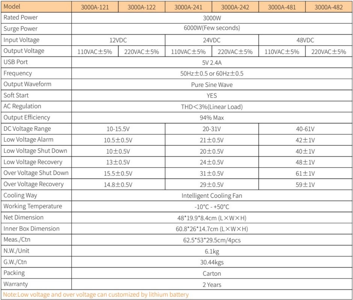
Product parameters

参数8 参数9 参数10 参数11 参数12 参数13

1. Design circuit diagram Before starting the production of the inverter PCB board, it is necessary to design the circuit diagram and determine the required electronic components and other components. Designing circuit diagrams requires professional technical and software support, usually completed by engineers or electronic experts. 2. Layout Layout refers to the process of placing electronic components on the inverter PCB board, which is one of the Committed step in the production of inverter PCB board. The correct layout can better organize electronic components and other components, making them easy to operate and maintain during welding. There are many ways of layout, which should be laid out reasonably based on the design of the circuit diagram and the actual situation. 3. Welding Welding is the final step in the process of inverter PCB components. The purpose of welding is to weld electronic components together with the solder pads on the inverter PCB board, ensuring stable and reliable connection and preventing component detachment. The welding process is divided into manual and automated methods, and the specific selection depends on factors such as the shape, size, and complexity of the inverter PCB board.

Product Details
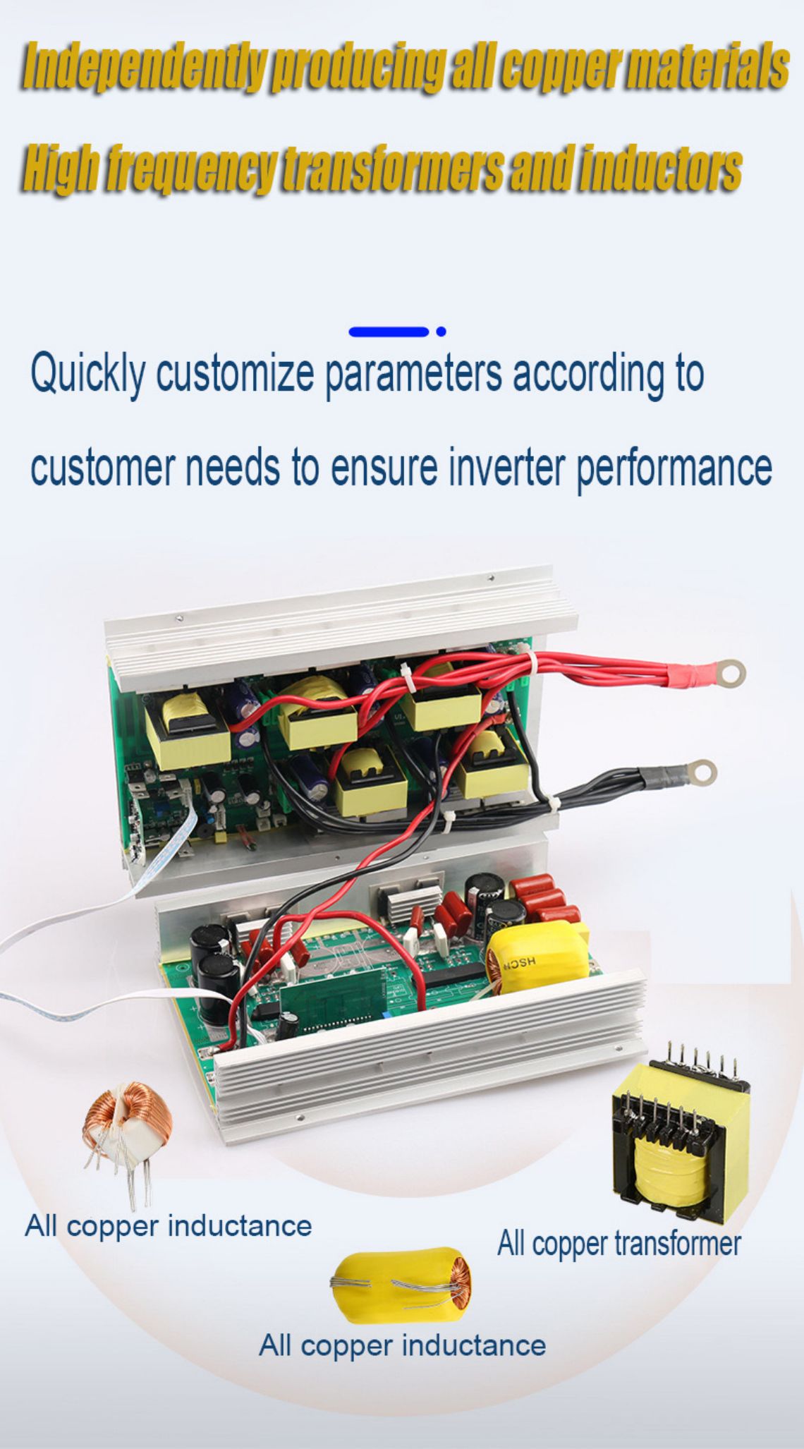
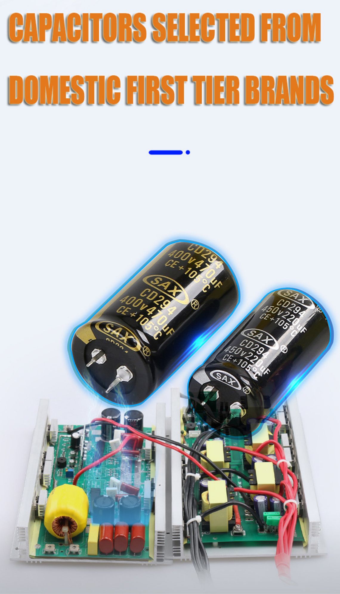
1. Design circuit diagram Before starting the production of the inverter PCB board, it is necessary to design the circuit diagram and determine the required electronic components and other components. Designing circuit diagrams requires professional technical and software support, usually completed by engineers or electronic experts. 2. Layout Layout refers to the process of placing electronic components on the inverter PCB board, which is one of the Committed step in the production of inverter PCB board. The correct layout can better organize electronic components and other components, making them easy to operate and maintain during welding. There are many ways of layout, which should be laid out reasonably based on the design of the circuit diagram and the actual situation. 3. Welding Welding is the final step in the process of inverter PCB components. The purpose of welding is to weld electronic components together with the solder pads on the inverter PCB board, ensuring stable and reliable connection and preventing component detachment. The welding process is divided into manual and automated methods, and the specific selection depends on factors such as the shape, size, and complexity of the inverter PCB board.

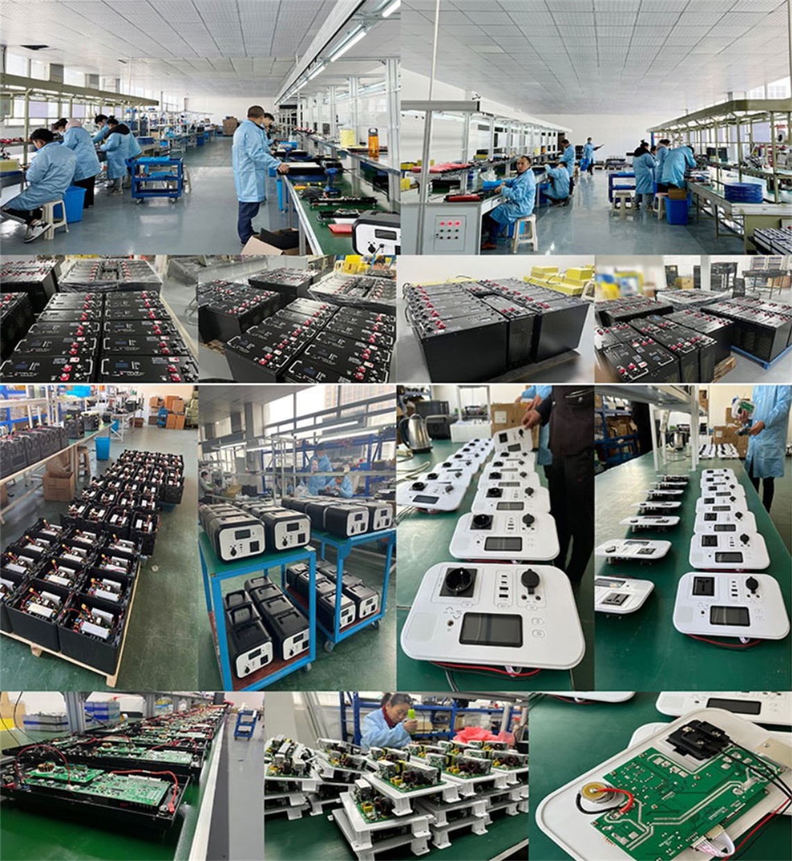
Workshop

Portable outdoor emergency power station

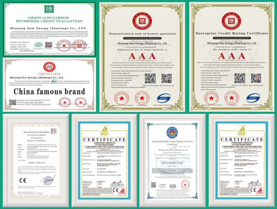
Certificate

Portable electric vehicle charging station

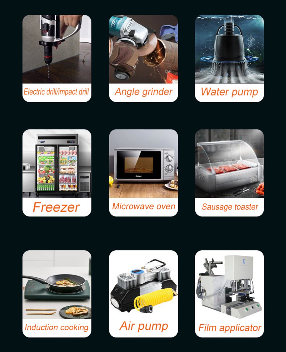
Product application cases

High Frequency  pure sine wave inverter

Transportation and packaging

Electric vehicle charging station

FAQ

Q:What is the name of your company?
A:Minyang new energy(Zhejiang) co.,ltd
Q:Where is your company?
A:Our company is located in Wenzhou, Zhejiang, China, the capital of electrical appliances.
Q:Are you a directly factory or trading company?
A:We are outdoor power supply manufacturer.
Q: How does your factory do regarding quality control?
A: Quality is the priority. We always attach great importance to quality
controlling from the start to the end. All our products have gained CE, FCC, ROHS certification.
Q:What can you do?
A:1.AII of our products have proceeded aging test before shipment and we guarantee safety while using our products.
2. OEM/ODM orders are warmly welcomed!
Q:Warranty and return:
A:1. Products have been tested by 48hours continuous load aging before ship out.wanrranty is 2 years
2. We own the best after-sale service team, if any problem happens, our team will do our best to solve it for you.
Q:Is sample available and free?
A:Sample is available, but the sample cost should be pay by you. The cost of sample will be refund after further order.
Q:Do you accept customized order?
A:Yes, we do.
Q:What's the delivery time?
A:It usually takes 7-20 days after confirming payment, but specific time should be based on tne order quantity.
Q:What are the payment terms of your company?
A:Our company supports L/C or T/T payments.

  • Previous:
  • Next:

  • Write your message here and send it to us